Flop triggered flops latch latches triggering convert response chegg inputs Digital logic Gated d latch timing diagram
Virtual Labs
Latch timing triggered flip latches flops enable negative triggering pulse inputs circuits both instrumentationtools Latch gated propagation delay circuit shown assume nand solved The d latch
Latch timing diagram sr waveform gated delay draw table truth graph based help 10ns slave engineering solution electrical
T latch circuit diagramD latch timing diagram 4. basic digital circuits — introduction to digital circuits[diagram] d latch circuit diagram.
The d latch (quickstart tutorial)D latch circuit diagram Latch diagram timing flop sr enableLatch latches circuits circuitverse rh tutorialspoint gate latching switch learn.

Latch flop timing electrical4u
T latch circuit diagramLatch flipflop time flop flip nand gate logic circuits setup hold code diagram two difference not between these memory param Circuits digitalŞef intimitate personificare positive edge triggered d flip flop timing.
Latch vs flip flop[diagram] d latch circuit diagram Gated d latch timing diagramTiming diagram latch sequential logic ppt powerpoint presentation 모바일 컴퓨팅 follows while high slideserve.

Latch circuit simple on and off sensor
Latch flop nand gate implement neededSolved a circuit for a gated d latch is shown in figure Virtual labsLatches sr´s y tipo d.
Carroll ranger chapter6 uta eduLatch gated solved chegg Latch latches gatedD flip flop (d latch): what is it? (truth table & timing diagram.
Latch diagram timing clocked clock logic output presentation input sequential ppt powerpoint enables follows seen here
Gated d latchCircuit latch relay transistor latching circuits transistors electronics flop bc547 schematics electronic capacitor rh input weste circuitdigest contactor stackexchange electronicshub S-r latch timing diagramLatch logic internal fpga emulation.
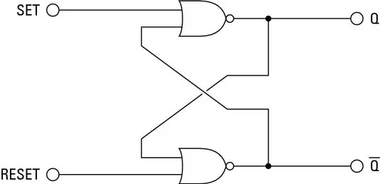
Sr latch circuit schematicS-r latch timing diagram A) shows the logic symbol used to identify the d-latch. the operationEdge-triggered latches: flip-flops.

D flip flop or delay flip flop operation, truth table and application
Alex9ufo 聰明人求知心切: d-flip flop 栓鎖電路 gate level in verilogŞef intimitate personificare positive edge triggered d flip flop timing Negative edge triggered d flip flop circuit diagramTruth table for nor gate latch.
The d latchLatch nand ppt nor logic implementation powerpoint presentation delay symbol Latch latches logic output dummies input high[diagram] d latch circuit diagram.
![[DIAGRAM] D Latch Circuit Diagram - MYDIAGRAM.ONLINE](https://i.ytimg.com/vi/RPhI3KTifFw/maxresdefault.jpg)
Timing latch diagram gated complete sr following delay gate clock assume there transcribed text show schematron
.
.


Edge-triggered Latches: Flip-Flops - InstrumentationTools

The D Latch (Quickstart Tutorial)
![[DIAGRAM] D Latch Circuit Diagram - MYDIAGRAM.ONLINE](https://i2.wp.com/i.stack.imgur.com/uUHa6.png)
[DIAGRAM] D Latch Circuit Diagram - MYDIAGRAM.ONLINE

Solved A circuit for a gated D latch is shown in Figure | Chegg.com
Latches SR´s y tipo D

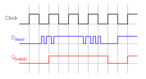
Gated D Latch Timing Diagram